Overview
From the time when NVIDIA released its first Fermi video card, the GeForce GTX 480, code named GF100, consumers have been wondering when they would see a full-out version of it. Now the time has finally arrived, the successor to the NVIDIA GeForce GTX 480, GeForce GTX 580, is making its debut. NVIDIA GeForce GTX 580 1.5GB, code named GF110, is the world’s fastest Direct X 11 GPU with an artistic design and screaming performance.
GTX 480 was never really challenged; it is a high-end graphic card, and GTX 580 just extends that lead in the single-GPU market to further bounds; it is a top-end graphic card.
It has high-end gaming performance and standards. To boost the performance, NVIDIA’s engineers took GF100 architecture and mainly optimized it for lower power consumption, better overall performance and greater efficiency all through the rendering pipeline. This revised GF100 architecture resulted in new GF110 architecture. This card is also the first in GeForce 500 series to use a totally enabled chip, which is based on the modified Fermi architecture, with all six 64-bit memory controllers active and all 16 stream multi-processors clusters.
Technical Specifications
| GPU Engine Specification | |
| CUDA Cores | 512 |
| Graphics Clock | 772 MHz |
| Processor Clock | 1544 MHz |
| Texture Fill Rate | 49.4 billion per sec |
| Memory Specification | |
| Standard Memory Config | 1536 MB GDDR5 |
| Memory Interface Width | 384-bit |
| Memory Clock | 2004 Mhz |
| Memory Bandwidth | 192.4 Gbps |
| Feature Support | |
| SLI Ready | 3-way |
| 3D Vision Ready | Yes |
| 3D Vision Surround Ready | Yes |
| PureVideo Technology | HD |
| PhysX Ready | Yes |
| CUDA Technology | Yes |
| Microsoft DirectX | 11 |
| OpenGL | 11 |
| Bus Support | PCI-E 2.0 x 16 |
| Certified for Windows 7 | Yes |
| Display Support | |
| Maximum Digital Resolution | 2560 x 1600 |
| Maximum VGA Resolution | 2048 x 1536 |
| Standard Display Connectors | Mini HDMI and Two Dual Link DVI |
| Multi Monitor | Yes |
| HDCP | Yes |
| HDMI | 1.4a |
| Audio Input for HDMI | Internal |
| Standard Graphic Card Dimensions | |
| Height | 4.376 inches (111 mm) |
| Length | 10.5 inches (267 mm) |
| Width | Dual-Slot |
| Thermal and Power Specifications | |
| Maximum GPU Temperature | 97 °C |
| Graphics Card Power | 244 W |
| Minimum Recommended System Power | 600 W |
| Supplementary Power Connectors | One 6-pin and One 8-pin |
Comparison between Radeon HD 6870 and GTX 580
| Graphic Cards | Radeon HD 6870 | GTX 580 |
| GPU Cores | 1120 | 512 |
| Shader Processor Clock | N/A | 1544 MHz |
| GPU Thermal Threshold | 105 °C | 97 °C |
| Graphics Clock (Core) | 900 MHz | 772 MHz |
| Peak Rasterization Rate | 900 Mtris/s | 3088 Mtris/s |
| Memory Size | 1024 MB | 1536 MB |
| Memory Interface | 256 bit | 384 bit |
| Memory Type | GDDR5 | GDDR5 |
| Memory Bandwidth | 134.4 GB/s | 192 GB/s |
| Memory Clock | 1050 MHz | 2004 MHz |
| Transistors | 1700 millions | 3000 millions |
| ROP Units | 32 | 48 |
| Texture Units | 56 | 64 |
| Peak Shader arithmetic | 2016 | 1581 |
| Power Consumption (idle) | 128 W | 150 W |
| Power Consumption (load) | 247 W | 363 W |
| Heat (idle) | 14 °C | 16 °C |
So, you can see that the GTX 580 delivers on much of what it promises.
Closer Look at the Design
GTX 580 is relatively more power efficient, cooler and quieter than its predecessor GTX 480. There were no issues with the GTX 480 gaming performance, but issues with performance per Watt though. NVIDIA has reengineered the GTX 580 at the transistor level (there are 3 Billion transistors) for better performance per Watt GPU. GPU core functions at 772 MHz rather than the 700 MHz of the GTX 480 1.5GB, with the 512 stream processors (SM) ripping along at 1,544 MHz rather than 1,400 MHz. Moreover, all 512 CUDA cores are enabled and active on this new architecture, while in GTX 480 cards only 480 CUDA cores were enabled.
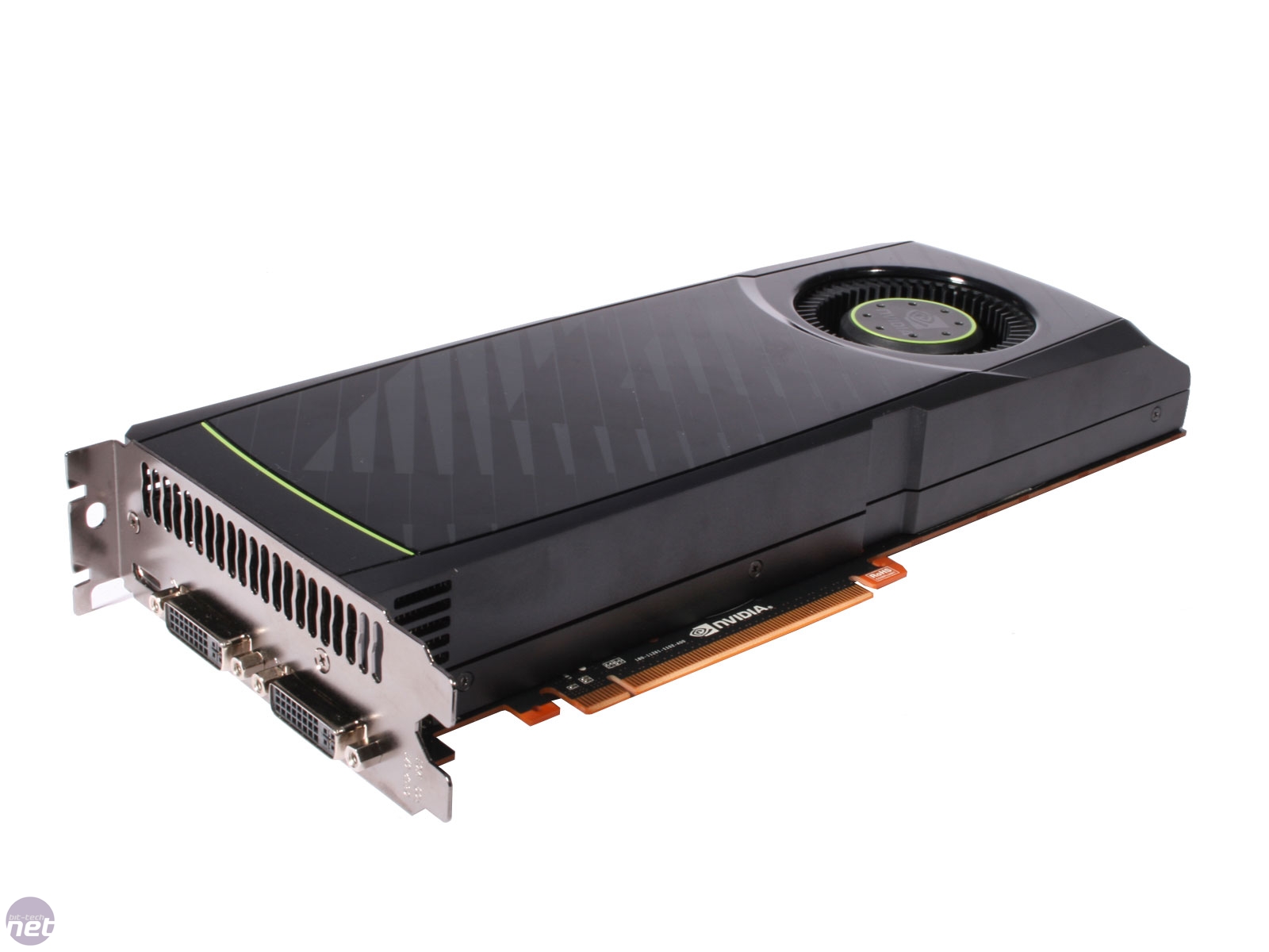
The GTX 580 Graphic Card, 26.7 cm in length, is quite good looking with the black colored monitor connectors. The card has two DVI port and one mini HDMI port. An interesting alteration to the GTX 580 circuitry is the inclusion of three small chips on the PCB, which is used for monitoring the power at the hardware level.
It uses a vapor-chamber technology heat plate to exploit heat transfer between the heatsink and the GPU. You can also see that the heatsink cools other components such as, memory chips and regulation circuitry. To offer the cooling of the GTX 580, the heatsink cover is somewhat lowered near the intake fan. The back of the card is very similar in appearance to its predecessor GTX480. There is a set of two SLI interconnections on the side, which provides a 3-way SLI support.
It has one 6-pin and one 8-pin power connectors, which are used for 250 Watts power supply to the card. The GDDR5 memory chips are manufactured by Samsung, and have the model number K4G20325FC-HC04 (1250 MHz) or K4G20325FC-HC03 (1500 MHz). NVIDIA uses a CHil CHL 8266 voltage regulator made in Thailand on their card. It offers extensive voltage monitoring and control options using I2C, therefore it is a best option for ‘Overclockers’.
GF110 graphic processor is made up on a 40nm process and uses approximately 3.0 billion transistors (200 million less than GF100). The above silver metal surface is not the actual GPU; it is a heat spreader of the GPU. The actual GPU is fitted under the heat spreader, whose size is 520 mm2. The GF110 core is equipped with 64 texture units, 16 Polymorph engines, 512 CUDA cores, 1544Mhz on the CUDA cores, 16 streaming multiprocessors (SM), four Graphics Processing Clusters and48 ROP units with higher clock speeds of 772Mhz on the fixed function units.
GTX 580 is relatively more power efficient, cooler and quieter than its predecessor GTX 480. There were no issues with the GTX 480 gaming performance, but issues with performance per Watt though. NVIDIA has reengineered the GTX 580 at the transistor level (there are 3 Billion transistors) for better performance per Watt GPU. GPU core functions at 772 MHz rather than the 700 MHz of the GTX 480 1.5GB, with the 512 stream processors (SM) ripping along at 1,544 MHz rather than 1,400 MHz. Moreover, all 512 CUDA cores are enabled and active on this new architecture, while in GTX 480 cards only 480 CUDA cores were enabled.
The GPU maintains the same six 64-bit GDDR5 memory controllers to facilitate high bandwidth access to the frame buffer. The GPU architecture is designed to facilitate more pervasive use of the GPU for solving parallel problems. All threads that access the same memory locations at runtime automatically run faster, due to availability of a global L2 cache and 48 KB of L1 cache per SM.
The Bottom Line
NVIDIA GeForce GTX 580, the fastest single GPU card on planet, is what all hardcore gamer had been waiting for. You can play any game out there and defend its territory with impunity. NVIDIA’s 3DVision Surround and system technology needs to be seen to be believed for a 3D Surround experience. There is a remarkable amount of efficient performance in the GTX 580. They have improved the fan noise, making it quietest card in the 3D load.
The card is blistering fast, particularly in newer DirectX 11 technology. There is no doubt that it is a better performing video card than the AMD’s Radeon HD 5870, but its real competition is going to be the Radeon HD 6900 series. However, I think that it will go head-to-head with the upcoming AMD series.
GeForce GTX580 is costly, but price doesn’t matter if you are an ultra-rich game enthusiasts. Only problem is a lack of Display Port connector, offering one mini HDMI port and two DIV ports instead. If we put this aside, NVIDIA has managed an impressive feat.
It is a very desirable and impressive graphics card; better on every aspect that consumers had issues with.